|
TopNax |



Intel’s Second-Gen Core CPUs: The Sandy Bridge Review |
|
Although the processing cores in Intel’s Sandy Bridge architecture are decidedly similar to Nehalem, the integration of on-die graphics and a ring bus improves performance for mainstream users. Intel’s Quick Sync is this design’s secret weapon, though. Editor’s Note: Eager to show off what is has done with Intel’s Sandy Bridge architecture, system builder CyberPower PC is offering Tom’s Hardware's audience the opportunity to win a new system based on Intel’s Core i7-2600K processor. Read through our review, and then check out the last page for more information on the system, plus a link to enter our giveaway! The high-end desktop processor market is a one-horse race, with Intel’s LGA 1366-based Core i7-900-series CPUs pretty much tromping along uncontested. If you have the money and are building a performance-oriented machine, it’s hard to beat an overclocked Core i7-950. Power users who really need the punch of a six-core chip can go Core i7-970—just be ready to pay out the ears for the privilege of owning one. It’s the mainstream where we see more interesting battles being waged. Funny how healthy competition has a habit of forcing more aggressive prices, isn’t it? For example, the quad-core Core i5-760 is compelling at $200. But so is AMD’s six-core Phenom II X6 1075T. And while AMD’s Black Edition parts captured the hearts of overclocking enthusiasts long ago, Intel more recently shipped a couple of K-series SKUs that bucked the company’s habit of only unlocking the multipliers on thousand-dollar Extreme Edition parts.
And now we have a new architecture from Intel, called Sandy Bridge. The last time Intel launched a processor design, it started with high-end Core i7-900-series chips and let the technology trickle down to the mainstream and entry-level derivatives. This time is different. Sandy Bridge is going to have to swim its way upstream, surfacing on the flagship LGA 2011 interface in the second half of this year for the real workstation-oriented aficionados.
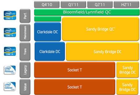
That’s a long way away, though. Between now and then, LGA 1366 is supposed to remain at the top of Intel’s stack, while LGA 1155-based processors centering on Sandy Bridge gobble up all of the volume as a result of what Intel claims is a ~30% performance improvement versus the Lynnfield- and Clarkdale-based processors. Naturally, this means trouble for an AMD that continues to launch incrementally faster versions of its existing architecture—but nothing that’d give it the double-digit speed-up needed to fend off a new microarchitecture from its competition. The only way to strike back at this point is with lower prices, and that's probably not the route AMD wants to be taking. We expect Bulldozer, the company's own next-gen architecture, sometime in 2011; that launch can't come soon enough.
A large enough boost from Sandy Bridge would also make Intel’s Core i7-900-series vulnerable too, though. Right now, these are, at minimum, $300 parts (that’s just to get in the door with a -950) that drop into generally more expensive motherboards requiring pricier triple-channel memory kits. I’ve been saying all along that the X58 platform would remain, definitively, Intel’s crown jewel on the desktop. But after running the numbers I’ve run on Sandy Bridge, I have to wonder if X58’s days are numbered a little sooner than the company planned. Sandy Bridge has a couple of other surprises up its sleeve—not all of them destined to go down as smoothly as a 1996 Dom Perignon on New Year’s Eve. For one, overclocking on an Intel platform is drastically different, and the LN2-drinking crowd probably won’t like it very much. There’s also a big emphasis on integrated graphics, which we’ve seen prematurely praised as a potential alternative to entry-level discrete graphics. That doesn't turn out to be the case, at least on the desktop.
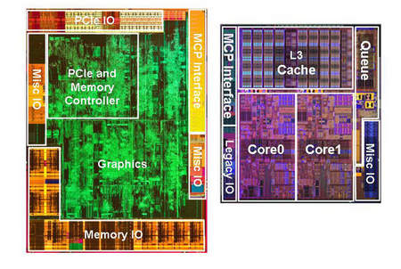
Intel's year-old Clarkdale multi-chip package.
The new hotness: Sandy Bridge, now with more integration.
On the other hand, Sandy Bridge comes armed with a block of fixed function logic that specifically addresses video encoding. AMD and Nvidia have no answer to this, are a year behind Intel with a competitive solution, and get completely outperformed today in video workloads. We also have a couple of unlocked SKUs that really give this architecture, manufactured at 32 nm, room to stretch its legs. Putting Sandy Bridge To The Test Leading up to the Sandy Bridge architecture’s launch, Intel sent over four SKUs from its upcoming lineup: Core i7-2600K, Core i5-2500K, Core i5-2400, and Core i3-2100. We put all four processors through a brand new benchmark suite for 2011, along with Bloomfield-, Lynnfield-, Clarkdale-, and Yorkfield-based chips from Intel, plus Thuban- and Deneb-based CPUs from AMD. While many of you were enjoying time away from work around Christmas and digging out of blizzard-like conditions ahead of New Year's Eve, the Tom's Hardware Bakersfield, CA lab was kept busy and warm by the latest bleeding-edge CPUs being run through their paces. Shall we? |
Inside Of Sandy Bridge: Cores And Cache |
|
From 10 000 feet, the Sandy Bridge die you saw on the previous page looks like a complete departure from its predecessor. After all, the mainstream Clarkdale-based CPUs consisted of two physical chips—a dual-core CPU manufactured at 32 nm and a graphics core/integrated memory controller/PCI Express controller etched at 45 nm. Now we’re looking at a single 32 nm part with all of those capabilities crammed onto one piece of silicon. Drill down, though, and there are really a lot of similarities that turn out to be more evolutionary in nature.
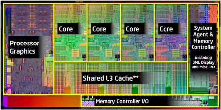
For each piece of Sandy Bridge that you look at, keep one word in mind: integration. Intel wanted to get the most out of each of the architecture’s nearly 1 billion transistors (the official count is 995 million). There are actually three different versions of the Sandy Bridge die shipping at launch. The quad-core configuration—the one composed of 995 million transistors—measures 216 mm². Then, there’s a dual-core die with 12 execution units making up its graphics engine. That one features 624 million transistors on a 149 mm² die. Finally, the slimmest variation sports two cores and a graphics engine composed of six EUs. Though it’s flush with 504 million transistors, you’d hardly know it given the 131 mm² die size. |
|
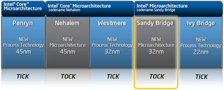
In comparison, the 45 nm Lynnfield design that served as the foundation for Intel’s Core i7-800- and Core i5-700-series chips measured a more portly 296 mm², despite the fact that it only consisted of 774 million transistors. Intel’s architects clearly owe much of what they were able to cram into Sandy Bridge to the engineers that brought the 32 nm node online for Westmere (tick), and then dialed in for today’s launch (tock). The Cores In its current state, Sandy Bridge-based processors are available with four cores (with and without Hyper-Threading) and two cores (dual-core models all have Hyper-Threading enabled). As you’ll see in the benchmarks, these cores are, clock-for-clock, more powerful than what we saw from Nehalem.
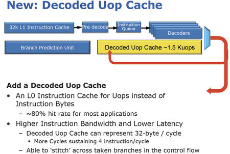
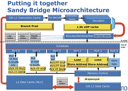
Still present are the 32 KB L1 instruction and data caches (along with 256 KB L2 cache per core), though Sandy Bridge now incorporates what Intel calls a L0 instruction cache that holds up to 1500 decoded micro-ops. This feature has the dual effect of saving power and improving instruction throughput. If the fetch hardware finds the instruction it needs in cache, it can shut down the decoders until they’re needed again. Intel also rebuilt Sandy Bridge’s branch prediction unit, improving its accuracy.
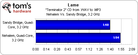
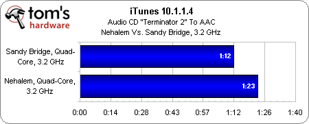
I ran these two single-threaded tests as a synthetic comparison of performance, clock for clock. Both quad-core chips are set to the same frequency with Turbo Boost and EIST disabled. As you can see, just the architectural shift makes a significant impact on Sandy Bridge's performance versus the Nehalem-based Lynnfield design. Sandy Bridge-based processors are the first to support Advanced Vector Extensions (AVX), a 256-bit instruction set extension to SSE (AMD will also support AVX in its upcoming Bulldozer processor architecture). The impetus behind AVX comes from the high-performance computing world, where floating-point-intensive applications demand more horsepower than ever. To that end AVX’s impact on Sandy Bridge will very likely be limited. Intel does, however, expect that audio processing and video editing applications should eventually be optimized to take advantage of AVX (along with the financial services analysis and engineering/manufacturing software that AVX is really designed to target). Unfortunately, there aren't any real-world apps optimized for AVX that we can test as a gauge of the capability's potential. Naturally, a lot of implementation work went into enabling AVX, including a transition from a retirement register file to a physical register. This allows operands to be stored in the register file, rather than traveling with micro-ops through the out-of-order engine. Intel used the power and die size savings enabled by the physical register to also significantly increase buffer sizes, more efficiently feeding its beefier floating-point engine.
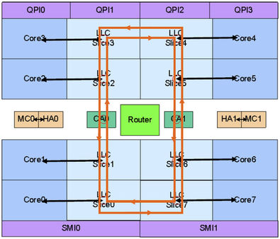
The Cache As a consequence of increased integration, Intel had to address the ways bits and pieces of its processor were accessing the last-level cache (in Sandy Bridge, it’s the L3). Back in the days of Bloomfield, Lynnfield, and Clarkdale, a four-core (and even six-core, in Westmere) ceiling meant that each physical core could have its own connection to that shared cache. The Xeon 7500-series processors were designed to be more scalable, though, and currently-shipping models feature as many as eight cores per CPU. Built the same way, that’d be an exorbitant number of traces between each core and the last-level cache. So, Intel adopted a ring bus that, in those enterprise environments, allows the company to keep scaling core count without the logistics getting out of control.
The ring bus, as it appears in Intel's Xeon 7500-series
Earlier this year, I had the chance to talk to Sailesh Kottapalli, a senior principle engineer at Intel, who explained that he’d seen sustained bandwidth close to 300 GB/s from the Xeon 7500-series’ LLC, enabled by the ring bus. Additionally, Intel confirmed at IDF that every one of its products currently in development employs the ring bus. Think we’re going to see a continued emphasis on adding cores and other platform components directly to the CPU die? I’d say that’s a fair assumption. Of course, Intel wasn’t worried about higher core count on the mainstream desktop version of Sandy Bridge. Rather, it was the on-die graphics engine that compelled a similar shift to the ring bus architecture, which now connects the graphics, up to four processing cores, and the system agent (formerly referred to as uncore) with a stop at each domain. Latency is variable, since each component takes the shortest path on the bus; overall, though it’s always going to be lower than a Westmere-based processor. At the end of the day, the ring bus’ most significant contribution is going to be the performance it facilitates in graphics workloads. |
The System Agent And Turbo Boost 2.0 |
|
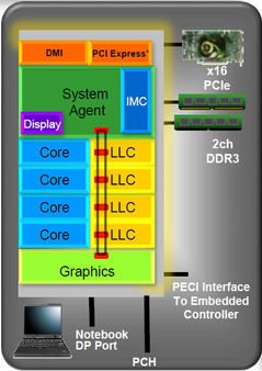
The System Agent Altered principally in name, the system agent includes functionality previously associated with the uncore—that is, it includes the processor subsystems that can’t be grouped with the execution cores (and now the graphics engine, too).
In that list, you have the dual-channel memory controller (which officially supports transfer rates of up to 1333 MT/s), 16 lanes of second-generation PCI Express connectivity, the DMI, and a more advanced power control unit, responsible for managing the operation of Turbo Boost, among its other roles. Turbo Boost 2.0? Speaking of Turbo Boost, Sandy Bridge includes a second-generation implementation of this technology, first seen two years ago on Bloomfield-based Core i7-900-series chips, but really only throttled up, so to speak, on Lynnfield a year later. The premise behind what I’ll call Turbo Boost 1.0 was that, in a multi-core CPU, available resources are not always in use. An application like iTunes, for instance, can only use one core at a time. And yet, the chip’s thermal ceiling is defined by a worst-case scenario of all cores fully-utilized. Turbo Boost takes advantage of the thermal headroom that exists when the chip executes a workload like iTunes, in turn accelerating the one active core to get its task completed faster. Turbo Boost 1.0 is smart in that it dynamically ratchets up the frequency of active cores based on temperature, current, power consumption, and operating system states. But it won’t exceed programmed power limits, even if thermal headroom exists to push performance harder.
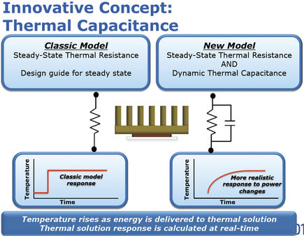
In the real-world, a processor doesn’t heat up right away, though. From idle, it takes time to reach its thermal ceiling. Turbo Boost 2.0 (or next-gen Turbo Boost, whatever you want to call it) allows the processor to exceed its power ceiling until it reaches its thermal limit, at which point it drops power to conform to those same programmed limits. Turbo Boost 2.0 does not mean the CPU will exceed its maximum Turbo Boost frequency. If you have a Core i7-2600K with a 3.4 GHz base clock and 3.8 GHz maximum Turbo clock, 3.8 is as fast as it’ll go in its stock trim. It’ll simply stay there longer—until the CPU heats up to its thermal limit—before backing down. Unfortunately, it’s not really possible to quantify the benefits of this capability. The best I could get out of Intel was that it helped improve responsiveness. On the desktop, I frankly wasn’t able to tell a difference, and as a result, Turbo Boost 2.0 comes across somewhat gimmicky. To be fair, it’s going to mean more in the mobile space, where base clocks start off a lot lower to save power, and Turbo Boost ceilings scale significantly higher. We have a Sandy Bridge-based notebook in the office and will be putting it through its pages this month, too.
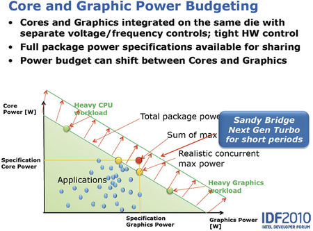
Also more impactful in the mobile space is Sandy Bridge’s ability to share thermal budget between graphics and processor cores. Previous-generation Arrandale cores were able to do this, applying the Turbo Boost concept to both components. Now Sandy Bridge enables the same capability on the desktop. Intel says that, in 3D-heavy workloads, the power control unit will bias to the graphics core, as it stands to improve performance more than faster CPU cores. |
Intel Core i7-875K And Core i5-655K Battle Beyond 4 GHz |
|
Do you like the idea of an unlocked clock multiplier, but don't want to pay $1,000 for an Extreme Edition? Intel's K-series CPUs bring overclocking down to the mainstream. The question is: can these scalable parts keep up with AMD's Black Edition CPUs? Editor's note: We're partnering up with CyberPower to give away a PC valued at $1,499 based on Intel's Core i7-875K processor. The contest details are on the last page of this review. Make sure you enter to win! Seven years ago, Intel was a rigid company. It vehemently discouraged overclocking—after all, that was just another way for unscrupulous resellers to liquidate lower-end processors as higher-margin parts. But then it let loose the Gallatin-based Pentium 4 Extreme Edition running at 3.4 GHz (not a far cry from where the 3.33 GHz Core i7-980X Extreme Edition sits today, in fact). Among the chip’s differentiating features was a 2MB L3 cache that added a bit of performance.
Over time, Intel did more to set the $1,000 Extreme Editions apart from the rest of its desktop lineup. Most notably, it granted the EEs unlocked clock multipliers, simplifying overclocking without officially sanctioning the practice. The problem: only someone willing to drop a grand got access to that nifty little feature. And really, how many of us have a spare thousand bucks lying around? Meanwhile, in an effort to excite enthusiasts (despite an overall performance disadvantage), AMD has, over the years, launched a number of Black Edition processors also armed with unlocked clock multipliers. Of course, the main difference between Intel's and AMD's efforts is that AMD’s unlocked parts are significantly cheaper. A Phenom II X2 550 Black Edition sells for less than $100. Even the company’s flagship Phenom II X6 1090T Black Edition sells for $310—less than a third of Intel’s Extreme Edition parts. Don’t get it twisted, though. AMD’s offerings cost less because they aren’t as fast at their stock speeds. You could even say that they’re priced competitively. It just so happens that overclockers don't really care about stock, default, or vanilla ice cream, though. They want to know what happens when you crank the dial, fire the afterburners, and add caramel sauce to the sundae that is a performance PC.
Intel Gets With The Program Because it’s seen as the company more sympathetic to the power user’s quest for control over his machine, many enthusiasts buy AMD-based hardware on principle. That's not the way I shop, but I read enough of the comments section to know what some of our most vocal readers think. Sure, Intel has loosened up over the years with high-end desktop SKUs, more flexible motherboards, and even the dual-socket Skulltrail platform. But the fact that its flashiest fare is also prohibitively expensive almost feels like a slap in the face to the very tenets of overclocking: garnering maximum value by optimizing affordable hardware, Celeron 300A-style. In an almost-unbelievable move, however, the company is giving enthusiasts something that AMD formerly had the monopoly on: reasonably-priced, unlocked parts that have the potential to overclock like hell. Meet the Core i7-875K and Core i5-655K. Aside from their K-designators and unlocked core/memory multipliers, both SKUs are exactly the same as processors already available today: Core i7-870 at 2.93 GHz and Core i5-650 at 3.2 GHz. Of course, the Core i7-875K centers on Intel’s 45 nm Lynnfield design, offering four cores with Hyper-Threading enabled, Turbo Boost technology, and a shared 8MB L3 cache. The chip’s dual-channel DDR3 memory controller is integrated onto the processor die, allowing it to move lots of data, quickly. According to Intel, the Core i7-875K employs the exact same silicon revision as previously-launched Lynnfield processors. |
|
The Core i5-655K leverages the 32 nm Clarkdale configuration, equipped with two physical cores that use Hyper-Threading to address four threads simultaneously. Turbo Boost is again made available, and the shared L3 cache drops to 4MB. Clarkdale sees the integrated memory controller moved off-die and onto another piece of silicon on the same package, which also houses onboard graphics. As expected, AES-NI acceleration makes a return here. Because both processors center on Intel’s LGA 1156 interface, you’re still limited to 16 lanes of on-package PCI Express 2.0 connectivity, potentially limiting the multi-card flexibility of these processors in a gaming rig. But we’re going to be testing with a single Radeon HD 5970 today. And for that dual-GPU board, 16 lanes is just the ticket… |
Intel: 4.8 GHz On Air? Sure! |
|
But that’s not the only curveball we’re throwing. It’d really be pointless to benchmark either of these new CPUs at their stock frequencies. Nobody pays a premium for an unlocked processor only to run it at the same speed as a couple of less expensive models. Instead, we’re pushing both chips as far as they’ll go on air (cooled by Noctua’s NH-D14, that is). The point here is to overclock via the unlocked multipliers, testing to see just how much headroom is available from Intel’s 45 nm and 32 nm nodes. Additionally, we’re adding a pair of Black Edition parts—the Phenom II X4 965 and Phenom II X6 1090T. The two AMD processors are priced at $185 and $310, respectively. Though Intel’s offerings are more expensive ($216 and $342), the quad-core Core i7-875K goes up against the six-core Phenom II X6 1090T fairly well, while the dual-core Core i5-655K takes on the quad-core Phenom II X4. Right out of the gate, AMD has the advantage on cost, so Intel has to prove itself in performance beyond 4 GHz. Core i7-875K Lynnfield’s “limitations” are fairly well-known, so it was hardly surprising to see the Core i7-875K reach a stable 4.13 GHz before exhibiting a bit of instability. We were actually able to run most tests at 4.26 GHz before determining that this CPU just couldn’t take the heat over the long term. Using Patrick’s Core i5 clock rate guide as a starting point, we got up to 1.5V before backing down and deciding 4.26 GHz just wasn’t going to happen. Naturally, heat was the enemy here, and CoreTemp saw us consistently butting up against the processor’s 99 degree Tj limit. Of course, it didn’t help that the fourth core ran particularly hot, cresting the limit as the other cores were just hitting 90 degrees. For all testing, Turbo Boost was disabled, giving us a static overclock. Hyper-Threading is left enabled, and Enhanced SpeedStep is on as well. Core i5-655K I was frankly most excited to work with the Core i5, a $216 part manufactured at 32 nm and set to run at 3.2 GHz by default. We’ve already had a couple of Clarkdale-based voltage-related fatalities here in the lab, so I wanted to exercise at least some caution. But ambition got the best of me and I ended up testing up to 1.45V—right about where Don lost his Pentium G6950.
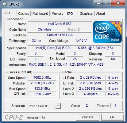
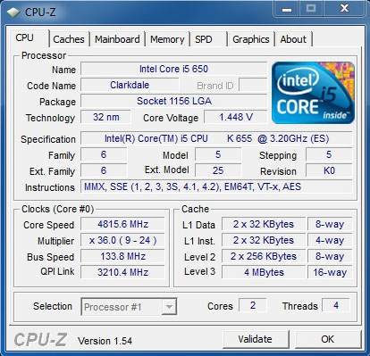
Nevertheless, I was able to boot at 4.93 GHz. On air. Without killing the chip. I managed to run a number of our benchmarks at 4.8 GHz, but crashing in 3ds Max 2010, for instance, compelled me to drop another notch to 4.66 GHz. Still, an extra 1.46 GHz isn’t bad (at a reduced voltage of 1.4165V).
Again, Turbo Boost was turned off for this one, with Hyper-Threading and SpeedStep turned on. As with the Core i7-875K, 8 GB of DDR3 memory ran at 1,066 MT/s with 7-7-7 timings. Really, the beauty of these unlocked parts is that you don’t have to worry about modules able to accommodate tons of headroom. Of course, if you have enthusiast-class DDR3, unlocked memory ratios let you scale data rates up and down (though there’s really little reason to go beyond the official 1,333 MT/s these chips support). |
|
Intel's Sandy Bridge Architecture |
|
|
Die Size (square mm) |
Transistors (million) |
|
Sandy Bridge (4C) |
216 |
995 |
|
Sandy Bridge (2C, HD Graphics 3000) |
149 |
624 |
|
Sandy Bridge (2C, HD Graphics 2000) |
131 |
504 |
|
Bloomfield (4C) |
263 |
731 |
|
Lynnfield (4C) |
296 |
774 |
|
Westmere (2C) |
81 |
383 |
|
Gulftown (6C) |
248 |
1168 |
|
Processor |
Base Clock Speed |
Unlocked Ratios |
Turbo Frequency |
Cores / Threads |
L3 Cache |
Memory |
TDP |
Price |
|
Core i7-980X |
3.33 GHz |
Core, DDR3, Power |
Up to 3.6 GHz |
6/12 |
12 MB |
3 x DDR3-1066 |
130W |
$999 |
|
Core i7-875K |
2.93 GHz |
Core, DDR3, Power |
Up to 3.6 GHz |
4/8 |
8 MB |
2 x DDR3-1333 |
95W |
$342 |
|
Core i7-860 |
2.8 GHz |
DDR3 (Up to 1,600 MT/s) |
Up to 3.46 GHz |
4/8 |
8 MB |
2 x DDR3-1333 |
95W |
$284 |
|
Core i5-655K |
3.2 GHz |
Core, DDR3, Power |
Up to 3.46 GHz |
2/4 |
4 MB |
2 x DDR3-1333 |
73W |
$216 |
|
Core i5-650 |
3.2 GHz |
None |
Up to 3.46 GHz |
2/4 |
4 MB |
2 x DDR3-1333 |
73W |
$176 |
