|
TopNax |
Radeon HD 6970 And 6950 Review: Is Cayman A Gator Or A Crock? |
|
Last month, Nvidia launched its GeForce GTX 580, but we told you to hold off on buying it. A week ago, Nvidia launched GeForce GTX 570 and we again said "wait." AMD's Cayman was our impetus. Were Radeon HD 6970 and 6950 worth the wait? Read on for more! In the world of high-end hardware, waiting for the next great thing means reading about a lot of technology and never actually buying a new piece of gear. That’s no way to enjoy your favorite games though, is it? Sometimes the wait is worth it, though. Last week was a perfect example. Nvidia launched its GeForce GTX 570, but we already knew AMD’s Radeon HD 6970 and 6950 boards had shipped out, FedEx Next Day Air. How could we not recommend waiting to see how these boards would compare? The very same morning, AMD launched a refresh on its Phenom II and Athlon II processors, incrementing clock rate. But we have Intel’s Sandy Bridge-based CPUs up and running in the lab. Again—why wouldn’t you wait a couple of weeks to see how they stack up?
Anticipating Greatness I was particularly interested in the performance of the Radeon HD 6970 and 6950, the two cards AMD had shipped so urgently. Whereas the Barts GPUs used to build Radeon HD 6870 and 6850 centered on the same VLIW5 architecture that earned Radeon HD 5870 a place in infamy, the Cayman GPU consolidates functionality into a VLIW4 design, incorporating fewer ALUs per thread processor, but improving performance per square millimeter of die space. How would that translate to the experience you get when you plug a 6900-series card into your system? Well, since Cayman is larger than Cypress, we have to assume it’s also going to be faster. A market populated by GF100-based boards like GeForce GTX 480 and GeForce GTX 470 would have made this launch so much easier for AMD. But Nvidia has this habit of kicking into gear when it really needs to. The resulting GeForce GTX 580 and 570 demonstrate that, even if Fermi remains a power-hungry architecture, it is possible to contend with more heat using a better sink and finely-tuned fan control. Suddenly, AMD had a much more daunting competitive landscape in front of it. We’re not sure if that was the real reason AMD’s Radeon HD 6900-series cards were delayed for nearly a month. However, the boards are here now (two of each, actually), and AMD claims that channel availability will be plentiful right out of the gate.
New GPU, Familiar Face AMD’s GPU team isn’t known for its bold, brash architectural moves—that honor belongs to Nvidia—so it’s hardly a surprise that much of Cayman looks familiar. In fact, there was no fancy press day hosted on an aircraft carrier to herald the improvements, nor were there conversations with chip architects. After the fanfare ahead of Radeon HD 6800, today's 6900-series launch was preceded by surprisingly little commotion. It was almost…refreshing. That gave us plenty of time to dig into the details for ourselves. Fortunately, we know enough about AMD's Cayman GPU to discuss what changes.
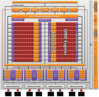
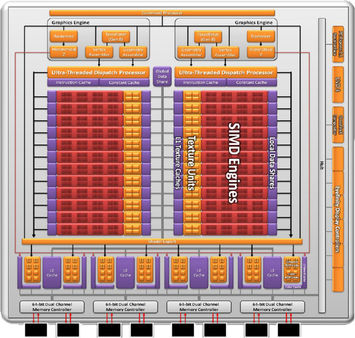
Fully loaded, the chip features up to 24 SIMD engines (up from Cypress’ 20). Each SIMD still includes 16 thread processors. Except now, each thread processor consists of four ALUs rather than five. So, while Cypress sported as many as 1600 ALUs, Cayman incorporates up to 1536 (that’s 24 * 16 * 4). Each SIMD engine is still tied to four texture units, totaling 96 on a complete Cayman chip (versus 80 on Cypress). |
|
12:00 AM - December 15, 2010 by Chris Angelini |
|
Look familiar? That's the 5870's Cypress |
|
Very similar: The 6900-series' Cayman |
|
As with the Cypress and Barts GPUs, Cayman is a product of TSMC’s now-mature 40 nm manufacturing process. It probably wouldn’t have been, but TSMC canceled its 32 nm node back in 2009, leaving both AMD and Nvidia to rethink their strategies. The aforementioned specs allowed AMD to keep its die size manageable, while still improving performance, though. Cayman is a 389 mm² piece of silicon composed of 2.64 billion transistors, while Cypress was 334 mm² part made up of 2.15 billion transistors. What AMD didn’t want to do was follow in Nvidia’s footsteps, creating a 500+ mm² behemoth that it’d need to power and then cool. From all angles, Cayman looks to be a compromise based on the hand TSMC dealt. It seems that the company was able to turn those lemons into something more palatable, though, by getting inventive with a feature called PowerTune, which balances TDP to facilitate higher shipping clock speeds. The two resulting board models, Radeon HD 6970 and 6950 handily outperform AMD’s last at-bat on the 40 nm process. The real question is, can they stack up to the more recent and renewed competition from Nvidia? Ten points, by the way, if you can figure out the reference in this story’s title.
|
Building Cayman By Improving Cypress |
|
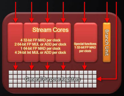
According to AMD, it had four principal design goals in building Cayman: more efficiency, improved geometry performance, new image quality features, and better power management. First, it wanted to create a more efficient graphics and compute architecture. The motivation behind this decision is sound enough—AMD was seeing a VLIW rate of roughly 3.4 in games. So, removing the special function transcendental unit and distributing its functionality across the other four units was actually a good performance per area optimization that promised to keep the GPU running within the observed operating rate. There are situations where performance could take a hit (when the VLIW utilization spikes above four), but AMD says that's unlikely. More important, AMD needed to create a more efficient architecture. Stuck on TSMC’s 40 nm manufacturing node, the company had to figure how to get more performance per millimeter of die space, rather than simply focusing on adding absolute performance. By shifting from its five-way VLIW architecture to a four-way design, AMD claims a 10% improvement to performance per square millimeter of die, as it’s able to add more SIMDs to the same amount of space.
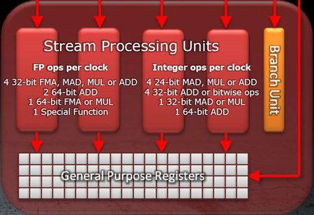
Streamlining the architecture doesn’t make it any less capable. The four stream processors now have identical capabilities, absorbing the special function unit’s role as well. In its VLIW4 configuration, each stream processor can do: · Four 32-bit FP FMA, MAD, MUL, or ADD per clock · Two 64-bit FP ADD per clock · One 64-bit FP FMA or MUL per clock · One FP Special Function per clock · Four 24-bit Int MAD, MUL, or ADD per clock · Four 32-bit Int ADD or bitwise opps per clock · One 32-bit Int MAD or MUL per clock · One 64-bit ADD per clock
Augmenting Compute Performance Although AMD’s compute-oriented aspirations are often taken less seriously than Nvidia’s, this does sound like an area that received some attention with Cayman. For instance, whereas the Radeon HD 5800-series cards perform double-precision math at one-fifth of the single-precision rate, Cayman operates at one-quarter the SP rate. Although the Radeon HD 6970’s peak single-precision rate is a touch lower than Radeon HD 5870 (2.7 TFLOPS versus 2.72 TFLOPS), you end up with 675 GFLOPS of peak double-precision math on the Radeon HD 6970 compared to 5870’s 544 GFLOPS. Note also that the Barts GPU sacrifices DP altogether, focusing on gaming performance rather than compute capabilities.
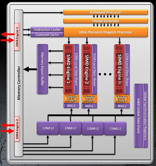
Cayman also incorporates dual bidirectional DMA engines, which ideally yield faster reads and writes to and from system memory over the PCI Express bus. Finally, AMD gives Cayman the ability to handle independent applications across the GPU. This is in contrast to Fermi, which can handle multiple kernels, so long as they’re spawned from the same CPU thread. Interestingly, that functionality isn’t part of DirectX 11, so AMD has to instead enable it through OpenCL sometime in the future. Aside from those functionality tweaks, Cayman retains Cypress’ cache structure. Each SIMD has its own 8 KB L1 cache for computational work, aside from the 16 KB L1 texture cache, plus a 32 KB local data share. Four 128 KB L2 caches continue keeping those SIMDs fed with information, and there is still a 64 KB global repository shared by all of the SIMDs. |
|
Cypress/Barts employs a VLIW5 architecture |
|
Cayman employs a more efficient/area VLIW4 configuration |
AMD Acknowledges That Geometry Matters |
|
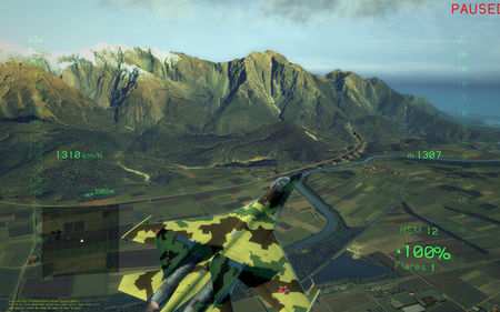
When Nvidia first briefed us on the gaming-oriented features of its Fermi architecture almost a year ago, it put the emphasis squarely on geometry. The company argued that modern GPUs have tons of shader performance—and we’d agree. For a flagship graphics card, we have to apply resolutions that most folks can’t even support and multiple monitor arrays just to tax performance. We aren't looking at photorealistic representations of our opponents' lower intestines in Call of Duty yet, but we’re certainly getting there. Unfortunately, the number of triangles per scene has not kept up. A mountain landscape might be peppered with very real-looking trees and grasses blowing in the wind, but the contours of the environment itself are distinctly geometric—not natural at all. The company purported to solve that issue with its PolyMorph engine—a tessellation unit in each Shader Multiprocessor that’d facilitate scalable performance when software developers started exploiting DirectX 11’s ability to dial up the geometric complexity of a scene.
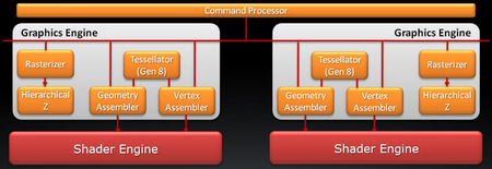
At the time, AMD responded that its own tessellation engine was more than capable of competing with Nvidia’s parallelized implementation. At the time, Unigine’s Heaven benchmark proved that to not be the case. Later, HAWX 2 gave us a real-world example of Nvidia’s architecture scaling better (though not as well as we might have expected, given Nvidia's insistence on the unit's scalability). With its Radeon HD 6900-series, AMD attempts to bridge the gap with a more focused stab at geometry. When we first looked at the Radeon HD 5870 more than a year ago, we observed that what AMD called dual rasterizers in its graphics engine was actually a rasterizer with a twice as many scan conversion units, upping the pixel throughput to 32 per clock. Now, with the 6900-series’ Cayman processor, you’re still looking at 32 pixels per clock from the rasterizer hardware. However, AMD essentially duplicated its geometry block in the new architecture (handling transform, setup, backface culling, and tessellation subdivision) adding a bit of load-balancing hardware to help with scaling. At the end of the day, Cayman can handle two triangles per clock, where Cypress (5800 series) and Barts (6800 series) could do one. Additionally, should Cayman’s on-chip caches overflow, as can happen when you’re talking about the extreme number of triangles associated with high tessellation factors, the additional vertices spill over to the frame buffer.
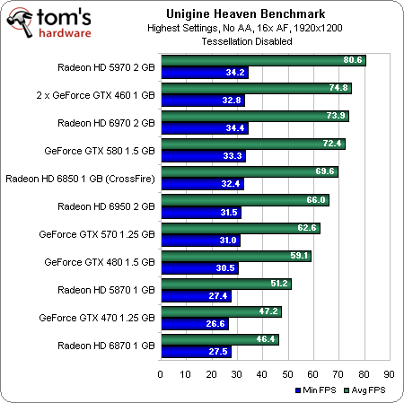
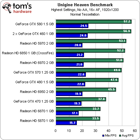
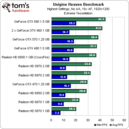
How does this translate into actual performance? Well, let’s start by running these cards through the same synthetic Unigine tests we’ve used in past reviews:
You can see the new cards do well with tessellation turned off—the 6970 even trumps Nvidia’s GeForce GTX 580. Increasing the tessellation factor hits the AMD boards incrementally harder, though, putting us in the eventual position where a GeForce GTX 480 outmaneuvers two 6850s in CrossFire. |
|
Cayman's Dual Graphics Engines |
|
Tessellation On: So much more realistic |
|
Tessellation Off: The mountains are so...geometric |
|
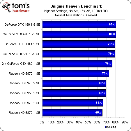
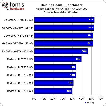
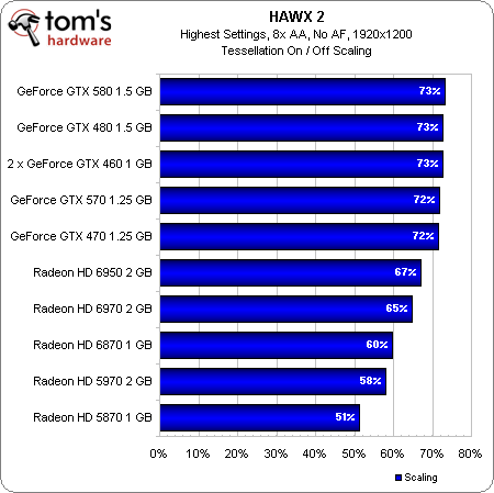
Get past the raw frame rates, though, and we can see that, while the Radeon HD 6900-series boards scale better than the 5800-series cards, improvements made to the Radeon HD 6800s seem to make more of a difference, as the Radeon HD 6870 tops the chart for AMD. Unfortunately for Cayman, that means Nvidia’s approach still yields a better scaling story.
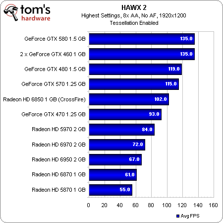
The performance in HAWX 2—really the only shipping game that uses tessellation to improve realism—isn’t much better for the 6900-series cards. The Radeon HD 6970 and 6950 bring up the bottom of the range behind cards like the GeForce GTX 570 and 470.
Check out the scaling chart, though. The Radeon HD 6970, despite losing out to all of Nvidia’s competing cards, comes a lot closer to matching the competition’s scaling profile here, and the Radeon HD 6950 does even better. It’s interesting that none of Nvidia’s GeForce boards scale based on the number of available PolyMorph engines. They all get stuck around 73% of their performance with tessellation turned on. This is almost assuredly what enables AMD’s cards to “catch up.” |
|
|
AMD Radeon HD 6970 |
AMD Radeon HD 6950 |
AMD Radeon HD 5870 |
Nvidia GeForce GTX 580 |
|
Manufacturing Process |
40 nm TSMC |
40 nm TSMC |
40 nm TSMC |
40 nm TSMC |
|
Die Size |
389 mm² |
389 mm² |
334 mm² |
520 mm² |
|
Transistors |
2.64 billion |
2.64 billion |
2.15 billion |
3 billion |
|
Engine Clock |
880 MHz |
800 MHz |
850 MHz |
772 MHz |
|
Stream Processors / CUDA Cores |
1536 |
1408 |
1600 |
512 |
|
Compute Performance |
2.7 TFLOPS |
2.25 TFLOPS |
2.7 TFLOPS |
1.58 TFLOPS |
|
Texture Units |
96 |
88 |
80 |
64 |
|
Texture Fillrate |
84.5 Gtex/s |
70.4 Gtex/s |
68 Gtex/s |
49.4 Gtex/s |
|
ROPs |
32 |
32 |
32 |
48 |
|
Pixel Fillrate |
28.2 Gpix/s |
25.6 Gpix/s |
27.2 Gpix/s |
37.1 Gpix/s |
|
Frame Buffer |
2 GB GDDR5 |
2 GB GDDR5 |
1 GB GDDR5 |
1.5 GB GDDR5 |
|
Memory Clock |
1375 MHz |
1250 MHz |
1200 MHz |
1002 MHz |
|
Memory Bandwidth |
176 GB/s (256-bit) |
160 GB/s (256-bit) |
153.6 GB/s (256-bit) |
192 GB/s (384-bit) |
|
Maximum Board Power |
250 W |
200 W |
188 W |
244 W |
